Designing a USB-C Power Delivery smart battery management board
Plug a USB-C charger into a laptop and it just works. Behind that simplicity is a small negotiation, a converter that has to decide whether to step voltage up or down, and a power path that keeps the system alive whether the battery is full, flat or missing. We recently designed, built and bench-validated a board that does all of that for a battery-powered product. We can’t talk about the product it serves, but we can talk about the engineering, and about the places where this kind of design tends to bite.
What the board has to do
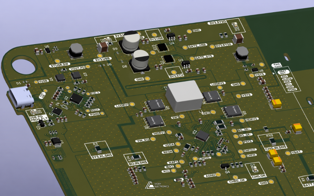
In one sentence: take power from a USB-C source, negotiate the right voltage, charge a multi-cell battery pack, feed the system from whichever source is available, and report every watt that moves along the way. In block form:
- Input: a USB-C Power Delivery sink controller with ESD protection on the connector.
- Conversion: an I²C-controlled buck-boost battery charger with a system power path.
- Distribution: a back-to-back MOSFET load switch for the system output, plus two independent 3.3 V buck converters combined through ideal-diode ORing.
- Supervision: a microcontroller with native USB, three power monitors, a temperature sensor, EEPROM storage, a hardware unique ID, a GPIO expander and buffered I²C links to the battery pack and to the host electronics.
Each block is well documented on its own. The difficulty is in the seams between them.
Hurdle 1: USB-C power is negotiated, not delivered
A plain USB-C port only gets 5 V. Anything more has to be requested over the CC lines, and the sink has to do that before any firmware is running, because the board may be starting from a flat battery. Standalone PD sink controllers solve this by loading their configuration from on-chip non-volatile memory at power-up. That is convenient, but it moves part of the design into a configuration step: the requested voltage profiles have to be correct before the board leaves the bench, and the vendor’s own documentation warns that this memory tolerates only a few thousand write cycles. It is not a scratchpad for experiments.
The connector is also the most exposed point on the board. We protected the CC and VBUS lines with dedicated USB-C protection and TVS devices, because a PD source can legitimately present up to 20 V on VBUS, which sits right next to the CC pins on a USB-C receptacle.
Hurdle 2: A charger that must be right before the MCU wakes up
A buck-boost charger is really two converters sharing one inductor, switching at hundreds of kilohertz through four external MOSFETs. Two things drive most of the layout effort:
- Hot loops and a thermal pad. The switching loops have to be tight, and the datasheet calls for the exposed pad to be soldered and stitched to the power ground planes with vias.
- Current sensing at the milliohm level. Input and charge current are measured across low-value sense resistors, and the datasheet requires an RC filter in the sense path to reject switching noise. A few millivolts of error there translates directly into a wrong current limit.
The part we like most about this class of charger is that its critical limits can be set in hardware. The battery cell configuration is selected by a resistor divider, and the input current limit is set by a pin voltage. The device then applies the lower of the pin setting and the register value. Getting those divider calculations right means the board is safe from the first power-up, even with blank firmware. We annotated each of those calculations directly on the schematic so the next engineer can check the maths without digging through our notes.
Hurdle 3: Keeping 3.3 V alive through every transition
The supervisory electronics must stay up while the cable is inserted, removed, or while the battery takes over. Instead of relying on one regulator, we generate 3.3 V twice, once from the USB input path and once from the battery side, and combine them with ideal-diode controllers driving external MOSFETs. Compared with Schottky ORing, this keeps the forward drop low and blocks reverse current between the rails. The system output goes through a back-to-back MOSFET switch with its own controller and an enable line, so the load can be disconnected under firmware control.
Hurdle 4: Buses that leave the board
I²C is easy until it runs through a connector to hardware that can be hot-plugged. A peripheral reset mid-transaction can hold SDA low forever, and live insertion can glitch a running bus. We placed hot-swap I²C buffers on both external links: one to the battery pack’s fuel gauge and one to the host electronics. The class of buffer we used pre-charges the lines to about 1 V before connecting, isolates bus capacitance, and, if a line stays low for around 40 ms, clocks out up to 16 pulses to free the stuck device.
Phantom powering is a quieter problem. When a powered board drives logic-high into an unpowered neighbour, current leaks through the neighbour’s input protection diodes and half-powers it. Engineering forums are full of reports of MCUs that fail to start for this reason. Our answer was open-drain buffers on the signals that cross to the host board, with the pull-ups on the receiving side, so no signal can supply power to a board that is switched off.
Hurdle 5: Measure everything
A smart BMS is only as smart as its telemetry. Three independent high-side monitors report voltage, current and power at the input, the battery and the system output, so firmware can close the energy balance and catch anomalies. A local temperature sensor, EEPROM for non-volatile storage, and a factory-programmed unique-ID EEPROM round it out. The unique ID lets the controller identify exactly which board is fitted, which pays off in production traceability and field support.
Layout: six layers, one side
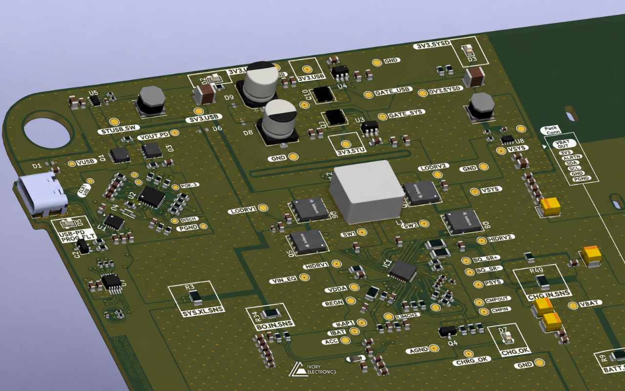
The final board is a six-layer design carrying over 500 footprints and more than 2,000 vias. An eight-layer, double-sided build was on the table early on; we settled on single-sided assembly, which generally keeps assembly simpler and cheaper. Power ground and digital ground are handled as separate nets and tied at a defined point, so switching currents stay out of the measurement and logic reference. We exported STEP models throughout, so the industrial design could keep pace with the electronics.
How we work
The project lives in KiCad as hierarchical sheets, one per functional block, under Git with branches and pull requests between engineers. The BOM carries assembly-house part numbers, so what we review is what gets placed. Reviews, calculations and design intent are kept next to the schematic, not in someone’s head.
The result
The boards were manufactured and validated on the bench: PD negotiation, battery charging, power-path switching and the full I²C sensor chain all working as designed.
If your product needs power delivery, battery management, precision measurement and embedded control on one board, and needs them to work together, that is exactly the kind of problem we enjoy solving. Get in touch at www.ivory-electronics.com.