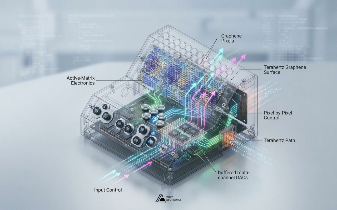
What it takes, electronically, to tell thousands of graphene pixels what to do
The terahertz band, sitting between microwaves and infrared light, is one of the last stretches of the electromagnetic spectrum that engineers cannot yet steer at will. That is changing. In an earlier post, we wrote about custom electronics that enable tunable reflection and transmission of THz light for imaging, sensing and communication. This time we want to go one level deeper into the electronics: how you drive a surface made of many independently controlled pixels, and why that turns out to be a very particular kind of circuit design problem.
The physics, as published
The scientific foundation comes from the group of Prof. Coskun Kocabas at the University of Manchester. In March 2025 the group published “Very-large-scale reconfigurable intelligent surfaces for dynamic control of terahertz and millimeter waves” in Nature Communications. The key ideas from the paper and the University’s announcement of it:
- The active layer is graphene on a thin polymer film, gated through an ionic-liquid electrolyte. Changing the charge density in the graphene changes how it interacts with THz and millimetre-wave radiation.
- No patterning is needed. The graphene sheet is continuous. Pixels are defined by the electrodes beneath it, so, as the team described it, the devices work “by adjusting local charge densities on a continuous graphene sheet, allowing for pixel-level control”.
- Scale comes from display technology. The published device uses a thin-film-transistor (TFT) backplane with more than 300,000 pixels over 12 × 9 cm², driven by a chip-on-glass display driver under the control of an external microcontroller.
- It works across a wide band. The paper reports operation from 100 GHz to 3 THz, with demonstrations including a single-pixel millimetre-wave camera using compressed sensing, dynamic beam steering, and beams carrying orbital angular momentum.
From an electronics engineer’s point of view, the most interesting sentence in the paper may be this one: “The scalability of our approach is primarily constrained by the capabilities of modern display technology.” In other words, the device is only as capable as the electronics that drive it.
Why a pixel is a capacitor
Electrically, each pixel is a small capacitor. An electrode on one side, graphene on the other, and an electrolyte in between that forms an electric double layer when a voltage is applied. That has three consequences for the driving electronics:
- Voltage sets the state. The optical behaviour of a pixel follows the voltage across it. Accurate, stable voltages mean accurate, repeatable pixel states.
- Charging takes time. Ionic gating is not instantaneous. The paper reports pixel charge and discharge times reduced to about 1 ms with short gate pulses of 30 µs. The drive timing has to respect that.
- The load is capacitive, everywhere. Every driver in the system sees capacitance: the pixel itself, the lines that reach it, and the transistors that switch it.

Active matrix, at PCB scale
Displays solved the problem of addressing huge numbers of pixels decades ago with the active matrix. Each pixel gets its own transistor acting as a switch. One set of lines drives the transistor gates and selects which pixels are listening. The other set of lines carries the voltage that should be written into them. When a pixel’s switch closes, its capacitor charges to the line voltage. When the switch opens, the pixel holds that charge while its neighbours are addressed.
The published work uses a TFT backplane fabricated on glass, the same technology behind LCD panels. Our board takes the same idea and builds it at printed-circuit-board scale, with discrete transistors: one per pixel, arranged in a row-and-column matrix, with one set of lines driving the gates and the other driving the drains. A PCB-level active matrix is not meant to compete with a display backplane on pixel count. What it offers is accessibility: a custom array can be designed, manufactured and modified far faster than a display backplane, with a pixel layout matched to a particular device or experiment. Every node can be probed, and there is no dependency on a display fab.
Analog lines, not just binary
The published system writes a binary voltage pattern: each pixel is driven to either a high or a low drain voltage, with the gate pulse width controlling the effective pixel voltage. Our board takes a different route. Every row and every column line is driven by its own channel of a multi-channel digital-to-analog converter (DAC). That means both the gate and drain voltages are set continuously under software control, not just switched between two rails. For experiments, this opens the door to greyscale pixel states, calibrated per-line voltages, and drive waveforms shaped in firmware rather than fixed by a driver IC.
A few architectural details make this work in practice:
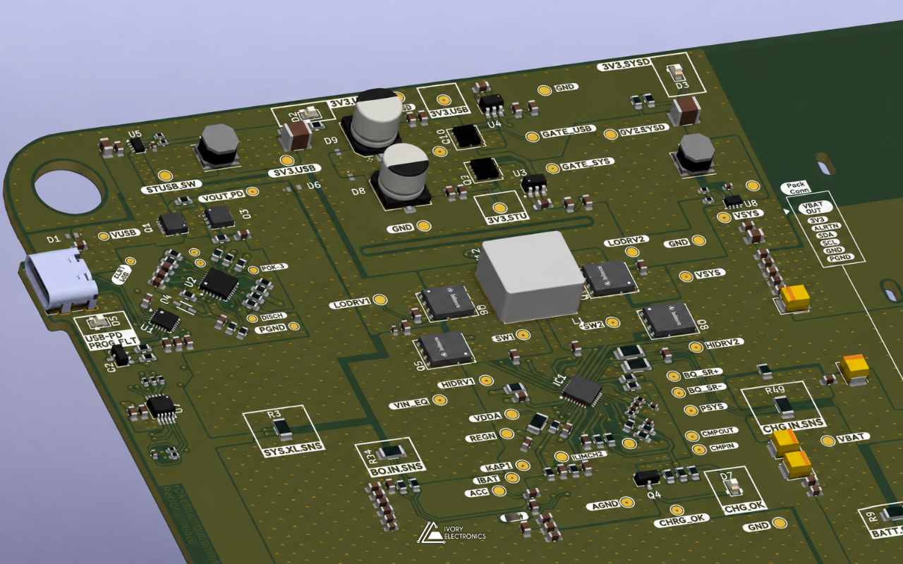
- Buffered outputs. Every DAC channel drives its line through an op-amp buffer, so the converters never see the line capacitance or a fault on the array side. Buffers on the gate lines use a small series resistor at the output. Analog Devices’ guidance on capacitive loading explains why: a series isolation resistor introduces a zero that “reduces the loop phase shift at higher frequencies”, keeping an op-amp stable when it drives capacitance.
- Synchronous updates. The DACs can load new values in the background and then update their outputs together with a dedicated load signal. A whole row and column pattern can therefore change at once, instead of rippling across the array channel by channel.
- Control-pin housekeeping. Reset, load and gain-select signals for every DAC are handled through an I²C port expander, so the host microcontroller’s pins are reserved for the fast SPI data path. Output gain can be set in firmware or fixed with on-board jumpers.
- Standalone addressing. Each DAC has its own chip select. Daisy-chaining would save wires, but independent addressing keeps the firmware straightforward on a first revision.
Designing for the device you do not have yet
One of the hardest parts of building electronics for novel devices is that the device is often not ready when the electronics are. We designed this board to be testable on its own:
- Optional dummy loads. Each DAC output has footprints for an RC network that emulates a capacitive pixel load. They are not fitted by default, but they let us check settling, stability and timing on the bench before a real device is attached.
- Test points everywhere they matter. Supplies, references and serial lines are brought out for probing.
- Ground partitioning. The digital I/O supply and the power path that feeds the DAC outputs and buffers return through separate ground domains, and the board provides a dedicated guard pad.
The pixel array itself was placed programmatically. When the same transistor-and-via cell must be repeated across the whole array at an exact pitch, a script is faster and far less error-prone than a mouse. The result is a six-layer board in which the array and its drivers were planned together from the start.
What makes this hard, and interesting
Driving a reconfigurable surface sits at an unusual intersection. Like a display, it needs dense, reliable addressing. Like precision instrumentation, it needs accurate, low-noise analog voltages. Like any electrochemical system, it needs respect for the device’s limits: an ionic-liquid electrolyte only tolerates a finite voltage window before unwanted reactions set in, so drive levels must be controlled and repeatable. And, like any research platform, it has to be flexible enough to support experiments nobody has thought of yet.
The paper itself highlights what is at stake. Reconfigurable surfaces like these can act as spatial light modulators to “dynamically steer THz light or to create complex beams, which is a critical capability required for next-generation communication systems.” Every one of those capabilities depends on getting the right voltage onto the right pixel at the right time.
The result
The board has been built and validated. It gives researchers a flexible, fully analog active-matrix platform for driving custom devices, one that can be adapted, probed and re-spun at the pace of research rather than the pace of a display fab.
If your team is developing a novel device that needs precision multi-channel drive electronics, whether for THz, optics, sensing or something entirely new, we would be glad to help. Visit www.ivory-electronics.com.
Ivory Electronics: Laying out ideas, tracing innovation.