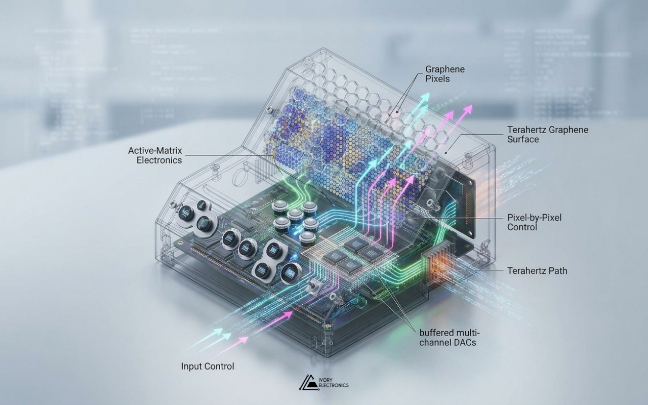
What it takes, electronically, to tell thousands of graphene pixels what to do The terahertz band, sitting between microwaves and infrared light, is one of the last stretches of the electromagnetic spectrum that engineers cannot yet steer at will. That is changing. In an earlier post, we wrote about custom electronics that enable tunable reflection and transmission of THz light for imaging, sensing and communication. This time we want to go one level deeper into the electronics: how you drive a surface made of many independently controlled pixels, and why that turns out to be a very particular kind of circuit design problem. The physics, as published The scientific foundation comes from the group of Prof. Coskun Kocabas at the University of Manchester. In March 2025 the group published “Very-large-scale reconfigurable intelligent surfaces for dynamic control of terahertz and millimeter waves” in Nature Communications. The key ideas from the paper and the University’s announcement of it: From an electronics engineer’s point of view, the most interesting sentence in the paper may be this one: “The scalability of our approach is primarily constrained by the capabilities of modern display technology.” In other words, the device is only as capable as the electronics that drive it. Why a pixel is a capacitor Electrically, each pixel is a small capacitor. An electrode on one side, graphene on the other, and an electrolyte in between that forms an electric double layer when a voltage is applied. That has three consequences for the driving electronics: Active matrix, at PCB scale Displays solved the problem of addressing huge numbers of pixels decades ago with the active matrix. Each pixel gets its own transistor acting as a switch. One set of lines drives the transistor gates and selects which pixels are listening. The other set of lines carries the voltage that should be written into them. When a pixel’s switch closes, its capacitor charges to the line voltage. When the switch opens, the pixel holds that charge while its neighbours are addressed. The published work uses a TFT backplane fabricated on glass, the same technology behind LCD panels. Our board takes the same idea and builds it at printed-circuit-board scale, with discrete transistors: one per pixel, arranged in a row-and-column matrix, with one set of lines driving the gates and the other driving the drains. A PCB-level active matrix is not meant to compete with a display backplane on pixel count. What it offers is accessibility: a custom array can be designed, manufactured and modified far faster than a display backplane, with a pixel layout matched to a particular device or experiment. Every node can be probed, and there is no dependency on a display fab. Analog lines, not just binary The published system writes a binary voltage pattern: each pixel is driven to either a high or a low drain voltage, with the gate pulse width controlling the effective pixel voltage. Our board takes a different route. Every row and every column line is driven by its own channel of a multi-channel digital-to-analog converter (DAC). That means both the gate and drain voltages are set continuously under software control, not just switched between two rails. For experiments, this opens the door to greyscale pixel states, calibrated per-line voltages, and drive waveforms shaped in firmware rather than fixed by a driver IC. A few architectural details make this work in practice: Designing for the device you do not have yet One of the hardest parts of building electronics for novel devices is that the device is often not ready when the electronics are. We designed this board to be testable on its own: The pixel array itself was placed programmatically. When the same transistor-and-via cell must be repeated across the whole array at an exact pitch, a script is faster and far less error-prone than a mouse. The result is a six-layer board in which the array and its drivers were planned together from the start. What makes this hard, and interesting Driving a reconfigurable surface sits at an unusual intersection. Like a display, it needs dense, reliable addressing. Like precision instrumentation, it needs accurate, low-noise analog voltages. Like any electrochemical system, it needs respect for the device’s limits: an ionic-liquid electrolyte only tolerates a finite voltage window before unwanted reactions set in, so drive levels must be controlled and repeatable. And, like any research platform, it has to be flexible enough to support experiments nobody has thought of yet. The paper itself highlights what is at stake. Reconfigurable surfaces like these can act as spatial light modulators to “dynamically steer THz light or to create complex beams, which is a critical capability required for next-generation communication systems.” Every one of those capabilities depends on getting the right voltage onto the right pixel at the right time. The result The board has been built and validated. It gives researchers a flexible, fully analog active-matrix platform for driving custom devices, one that can be adapted, probed and re-spun at the pace of research rather than the pace of a display fab. If your team is developing a novel device that needs precision multi-channel drive electronics, whether for THz, optics, sensing or something entirely new, we would be glad to help. Visit www.ivory-electronics.com. Ivory Electronics: Laying out ideas, tracing innovation.
Safely Configuring a Battery Fuel Gauge IC
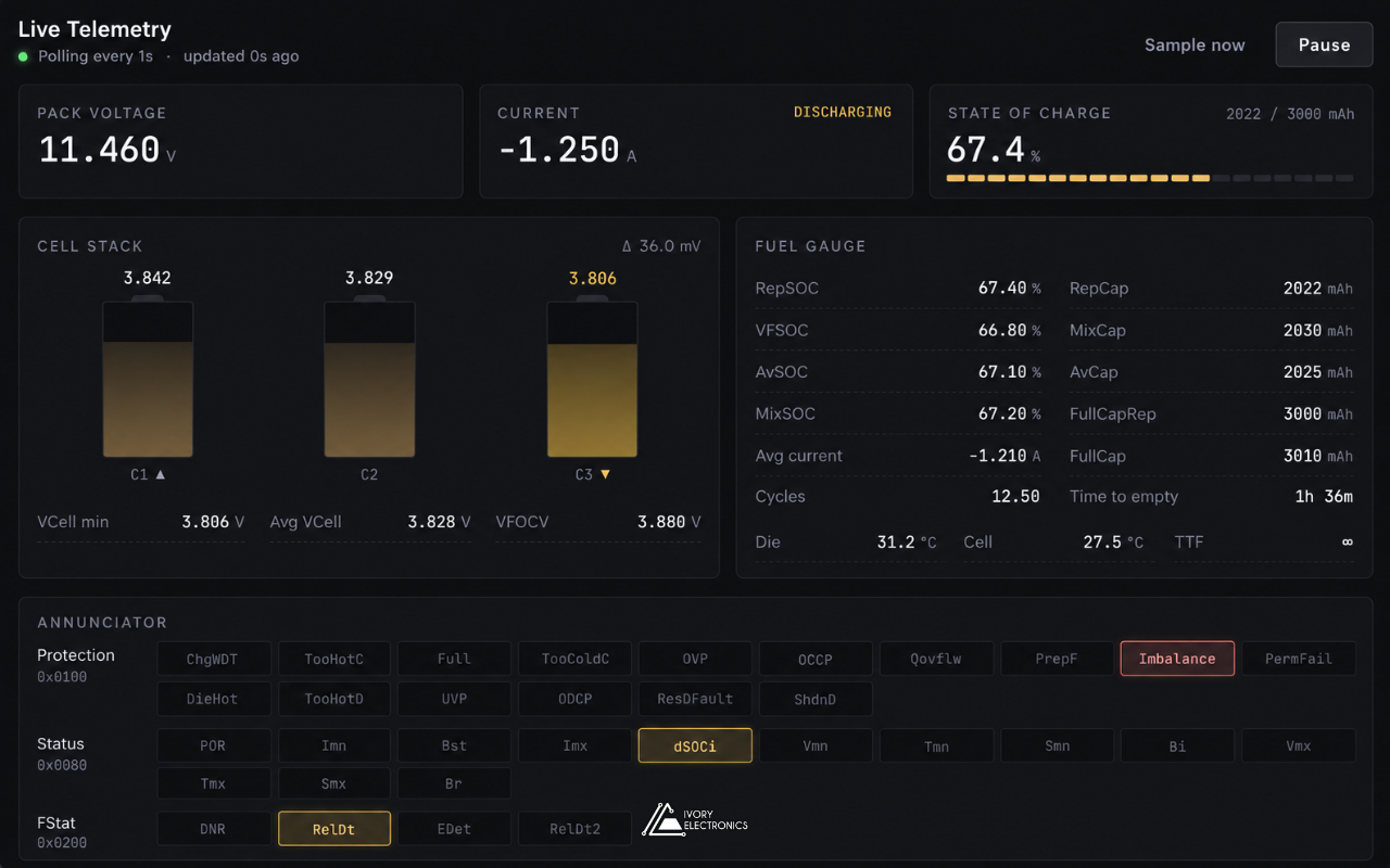
A desktop tool for a chip you can only program a handful of times A battery fuel gauge is the chip that tells a device how much charge is left. In many modern battery packs, the same chip also protects the cells against overvoltage, overcurrent and overheating. Its behaviour depends on a detailed configuration stored in on-chip memory. Getting that configuration right matters. A wrong value can make the state of charge drift, or make protection trip too early, or too late. And the memory that holds it can only be written a handful of times in the chip’s lifetime. So we built a desktop tool that makes battery fuel gauge configuration safe, visible and repeatable. What the tool does Hurdle 1: A memory you can only write a few times Most chips let you rewrite settings as often as you like. This one does not. Every permanent write uses up one of a small number of lifetime writes. Waste them, and the chip can no longer be updated. So the tool never writes permanent memory by accident. Changes go into the chip’s temporary working copy first. A soft reset then reloads the chip from that copy, so the new settings can be tested on real hardware as often as needed, without using a write. Only after testing does the commit step unlock. The operator must tick a confirmation box, and the button is disabled once no writes remain. A colour-coded gauge shows the remaining writes at all times: green is safe, amber means caution, red means almost none left. After a commit, the counter is read back from the chip to confirm it worked. Hurdle 2: Knowing exactly what will change A full configuration contains dozens of values. Writing all of them blindly is risky and hard to review. The compare view loads a configuration file and places it beside the values currently on the chip. Differences are highlighted, and a filter hides everything that already matches. The operator selects only the values that need to change, and writes just those. Hurdle 3: Raw registers mean nothing to people Inside the chip, everything is a 16-bit number. A voltage, a temperature and a status flag all look the same. The tool decodes each value into real units: volts, amps, milliamp-hours, per cent, degrees and time. Status and protection bits are turned into readable flags. The live view refreshes these values every second. Engineers can watch the battery fuel gauge respond as the pack charges or discharges, and check that a new configuration behaves as expected. Hurdle 4: Finding the hardware without fuss The chip sits behind a small microcontroller that acts as a USB bridge. Serial port names change between computers and cables, so asking the user to pick one is error-prone. On launch, the tool offers auto-connect. It scans the ports, finds the one that answers, confirms the chip is on the bus, reads the configuration and checks the write counter. Each step is shown on screen. If anything fails, it falls back to manual port selection with a clear error message. Keeping a record Configurations can be saved as named profiles, with a description, and exported as files for sharing or archiving. Profiles work offline, so a configuration can be prepared before the hardware is even on the bench. A log tab records every message between the app and the device. Entries are time-stamped to the millisecond and colour-coded by direction. The log length is capped, so long sessions stay fast. Under the hood The bridge speaks a simple, line-based text protocol, which makes it easy to debug and to extend. The same code builds native installers for macOS, Windows and Linux. Where it fits The tool supports both development and production. Engineers use it to tune and validate a battery fuel gauge configuration. The same tool then applies that proven configuration to each new pack, with the same checks every time. Working on battery fuel gauge configuration, battery pack production or custom engineering tools? We would like to hear about it. Visit www.ivory-electronics.com
Designing Electronics for the Edge of Space
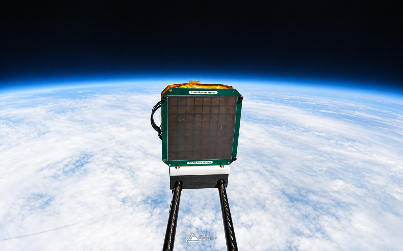
What it takes to fly a circuit board on a stratospheric balloon On 1 May 2023, a square green tile rode a weather balloon up through the atmosphere until the sky behind it turned black and the Earth’s horizon curved beneath it. The tile was SmartIR’s graphene smart radiator, and the flight was the company’s Mission 1, launched in collaboration with Sent Into Space. Behind the tile sat the circuit board that drove it, designed by our CEO, Dr. Daniel Melendrez, together with Prof. Coskun Kocabas of the University of Manchester. This post is about that board, and about what changes when the hardware you design is going to leave the ground. The mission, in public terms SmartIR is a University of Manchester spin-out developing graphene-based adaptive radiators: thin, lightweight devices that control how a surface emits heat, electronically and with no moving parts. That capability matters in space, where, as the ESA Business Incubation Centre UK has noted, satellites can experience temperature variations of more than 400 °C. Before orbit comes the stratosphere, and Mission 1 was the first time the technology left the lab. Our part was the electronics that sat between the payload’s controller and the multi-pixel tile. We will leave the device physics to SmartIR. What follows is the electronic design perspective: what the board had to be, and what the flight environment demanded of it. The requirements came down to a few words: The result is a six-layer board, about ten centimetres square, with fewer than 30 footprints, logos included. The revision code on the silkscreen reads Rev. A-0323: designed in March 2023, flying by May. Challenge 1: The cold In the International Standard Atmosphere, air temperature falls to about −56.5 °C at the tropopause and stays there for kilometres. That is below the −40 °C lower limit of the industrial temperature grade that most commercial parts are specified to. For a balloon payload, this means component ratings are the start of the conversation, not the end: Challenge 2: Almost no air Sent Into Space’s balloons typically climb to around 38 km before they burst. Up there, pressure is well under 1% of sea level, and convection, the mechanism most electronics quietly rely on to shed heat, all but disappears. Heat has to leave by conduction through the board and its mounting, or by radiation. There is a neat irony here: that is exactly the physics a radiator experiment is about, and the driver electronics are subject to it too. Keeping dissipation low and spreading it through copper planes is a design choice, not an afterthought, when the air cannot help. Challenge 3: The ride itself A balloon flight is not gentle. There is handling at launch, a long ascent, the burst at peak altitude, and a parachute descent to wherever the wind decides. Along the way the payload may pass through cloud layers where cold hardware can collect moisture. Flight-worthy electronics answer this with restraint: Challenge 4: The calendar Flight opportunities do not wait for a design to feel finished. This board went from revision A to launch in roughly two months. That puts a premium on getting it right first time: choosing well-documented parts, reading the datasheet’s fine print (one of the schematic notes is simply “Read pages 7 & 8 from Datasheet”), and building in configuration options so that small changes in requirements can be absorbed without a respin. The footprint nobody sells One of the more interesting parts of the design is not a component at all. The contact pattern between the board and the tile matches the tile’s own geometry, and no library in the world has it. It was generated by a script as a single custom footprint, with every contact positioned exactly and labelled for assembly and inspection. Programmatic generation means the geometry is consistent across the whole array, and a change to the tile becomes a parameter change rather than an afternoon of manual editing. It is a small example of a broader habit: when the tools do not have what the hardware needs, build the tool. Flight day SmartIR‘s own mission update is candid that the launch came “despite last-minute technical challenges”, and credits the teamwork between SmartIR and Sent Into Space for getting it off the ground. The driver board did its job: it flew on Mission 1 and drove the tile as intended, while SmartIR’s adaptive thermal tiles were, in the company’s words, “put to the test in near-space conditions”. Mission 1 was the first step. SmartIR has since taken its graphene radiator to low Earth orbit, launching on SpaceX’s Transporter-12 in January 2025 and on Transporter-13 in March 2025. What we took from it Hardware for a flight test is an exercise in restraint. The best decisions on this board were the ones that removed things: fewer wires, fewer parts, no moving configuration, and a power-up state that does nothing until it is told to. The same instincts shape everything we build at Ivory Electronics, whether it is headed for the stratosphere or a lab bench. If you are developing a novel device that needs electronics to drive it, test it or take somewhere unusual, we would be glad to help. Find us at www.ivory-electronics.com
One Cable In, Every Rail Accounted For
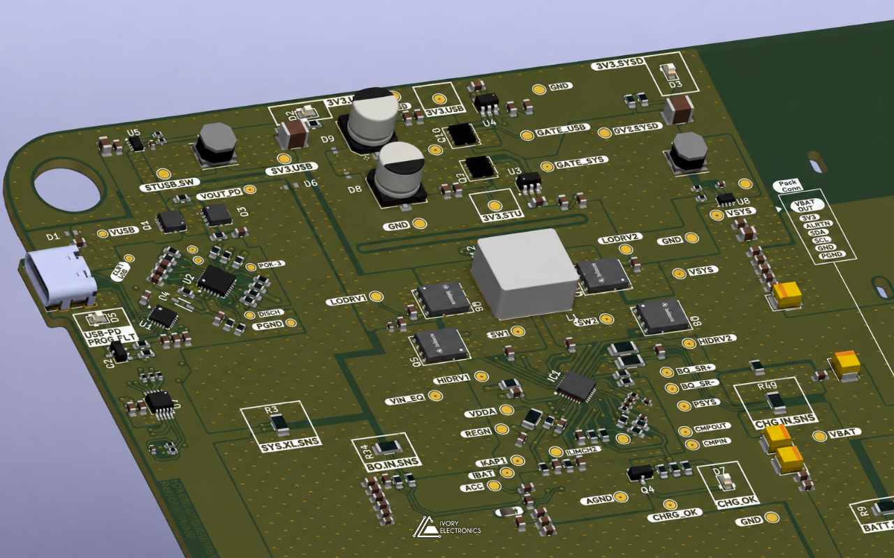
Designing a USB-C Power Delivery smart battery management board Plug a USB-C charger into a laptop and it just works. Behind that simplicity is a small negotiation, a converter that has to decide whether to step voltage up or down, and a power path that keeps the system alive whether the battery is full, flat or missing. We recently designed, built and bench-validated a board that does all of that for a battery-powered product. We can’t talk about the product it serves, but we can talk about the engineering, and about the places where this kind of design tends to bite. What the board has to do In one sentence: take power from a USB-C source, negotiate the right voltage, charge a multi-cell battery pack, feed the system from whichever source is available, and report every watt that moves along the way. In block form: Each block is well documented on its own. The difficulty is in the seams between them. Hurdle 1: USB-C power is negotiated, not delivered A plain USB-C port only gets 5 V. Anything more has to be requested over the CC lines, and the sink has to do that before any firmware is running, because the board may be starting from a flat battery. Standalone PD sink controllers solve this by loading their configuration from on-chip non-volatile memory at power-up. That is convenient, but it moves part of the design into a configuration step: the requested voltage profiles have to be correct before the board leaves the bench, and the vendor’s own documentation warns that this memory tolerates only a few thousand write cycles. It is not a scratchpad for experiments. The connector is also the most exposed point on the board. We protected the CC and VBUS lines with dedicated USB-C protection and TVS devices, because a PD source can legitimately present up to 20 V on VBUS, which sits right next to the CC pins on a USB-C receptacle. Hurdle 2: A charger that must be right before the MCU wakes up A buck-boost charger is really two converters sharing one inductor, switching at hundreds of kilohertz through four external MOSFETs. Two things drive most of the layout effort: The part we like most about this class of charger is that its critical limits can be set in hardware. The battery cell configuration is selected by a resistor divider, and the input current limit is set by a pin voltage. The device then applies the lower of the pin setting and the register value. Getting those divider calculations right means the board is safe from the first power-up, even with blank firmware. We annotated each of those calculations directly on the schematic so the next engineer can check the maths without digging through our notes. Hurdle 3: Keeping 3.3 V alive through every transition The supervisory electronics must stay up while the cable is inserted, removed, or while the battery takes over. Instead of relying on one regulator, we generate 3.3 V twice, once from the USB input path and once from the battery side, and combine them with ideal-diode controllers driving external MOSFETs. Compared with Schottky ORing, this keeps the forward drop low and blocks reverse current between the rails. The system output goes through a back-to-back MOSFET switch with its own controller and an enable line, so the load can be disconnected under firmware control. Hurdle 4: Buses that leave the board I²C is easy until it runs through a connector to hardware that can be hot-plugged. A peripheral reset mid-transaction can hold SDA low forever, and live insertion can glitch a running bus. We placed hot-swap I²C buffers on both external links: one to the battery pack’s fuel gauge and one to the host electronics. The class of buffer we used pre-charges the lines to about 1 V before connecting, isolates bus capacitance, and, if a line stays low for around 40 ms, clocks out up to 16 pulses to free the stuck device. Phantom powering is a quieter problem. When a powered board drives logic-high into an unpowered neighbour, current leaks through the neighbour’s input protection diodes and half-powers it. Engineering forums are full of reports of MCUs that fail to start for this reason. Our answer was open-drain buffers on the signals that cross to the host board, with the pull-ups on the receiving side, so no signal can supply power to a board that is switched off. Hurdle 5: Measure everything A smart BMS is only as smart as its telemetry. Three independent high-side monitors report voltage, current and power at the input, the battery and the system output, so firmware can close the energy balance and catch anomalies. A local temperature sensor, EEPROM for non-volatile storage, and a factory-programmed unique-ID EEPROM round it out. The unique ID lets the controller identify exactly which board is fitted, which pays off in production traceability and field support. Layout: six layers, one side The final board is a six-layer design carrying over 500 footprints and more than 2,000 vias. An eight-layer, double-sided build was on the table early on; we settled on single-sided assembly, which generally keeps assembly simpler and cheaper. Power ground and digital ground are handled as separate nets and tied at a defined point, so switching currents stay out of the measurement and logic reference. We exported STEP models throughout, so the industrial design could keep pace with the electronics. How we work The project lives in KiCad as hierarchical sheets, one per functional block, under Git with branches and pull requests between engineers. The BOM carries assembly-house part numbers, so what we review is what gets placed. Reviews, calculations and design intent are kept next to the schematic, not in someone’s head. The result The boards were manufactured and validated on the bench: PD negotiation, battery charging, power-path switching and the full I²C sensor chain all working as designed. If your product needs power delivery, battery management, precision measurement and embedded control on one
From Probe to Screen: Building an All-in-One Electrochemistry Bench
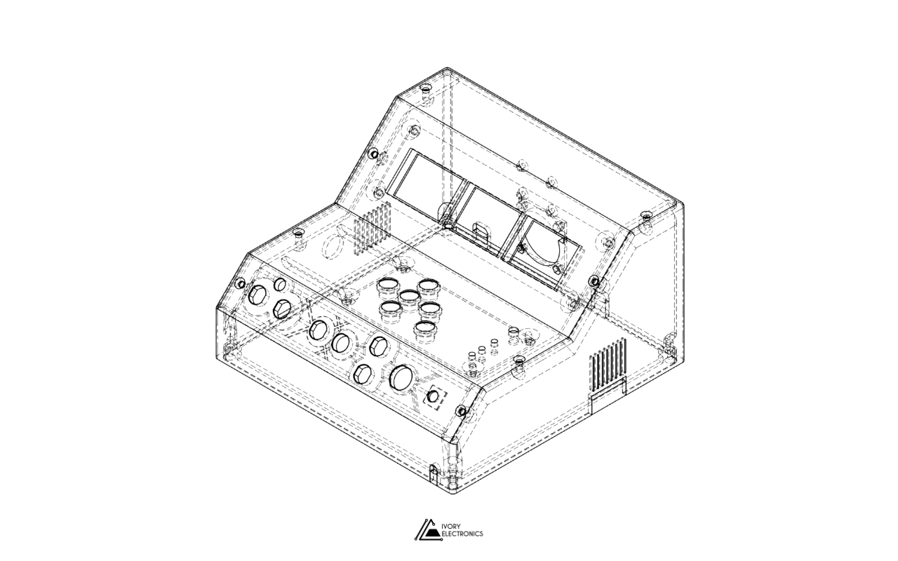
Designing an integrated instrument for the teaching and research lab In many labs, an electrochemistry experiment still means a familiar scene: a bench supply, a multimeter or two, a conductivity meter, a thermometer, and a tangle of leads connecting them. Every instrument has its own display, its own quirks and its own way of recording (or not recording) data. We were asked to fold that bench into one instrument for university-level teaching and research work. The electronics are designed, built and validated on the bench. Here is what went into it, and why it was harder than it looks. One box, many jobs The instrument brings together, on a single two-layer board: Each function is textbook on its own. Making them coexist on one board, sharing one supply, is where the engineering happens. Hurdle 1: Mixed-signal on two layers A two-layer board keeps cost down, but it removes the luxury of a solid ground plane under everything. Here, a power stage that can carry hundreds of milliamps shares the board with millivolt-level measurement signals. We split the design into three ground domains (analog, digital and power) and joined them deliberately with net ties, so return currents from the output stage and the digital logic do not flow through the analog reference. The design is organised into digital and analogue sections, keeping the sensitive front ends away from the power paths. Power comes in over USB-C Power Delivery, negotiated at 12 V, with a TVS clamp at the input and a supply-health signal back to the controller. From there, dedicated regulators generate the logic rails, separate analog rails and a symmetric ± supply for the circuits that need to swing both sides of ground. Hurdle 2: A current limit that has to survive itself Electrochemical cells are unforgiving loads: an electrode short or a misconnected lead can ask for far more current than the experiment needs. The output therefore has a real current clamp: a sense resistor, an error amplifier and a MOSFET that regulates linearly to hold the current at a limit that the firmware sets through a DAC. A separate comparator watches for overload and raises a digital flag, which firmware turns into an audible alarm. The catch with linear regulation is heat. At the limit, the MOSFET absorbs the entire difference between the supply and the load voltage. Semiconductor vendors warn that linear-mode operation is exactly where MOSFETs are most fragile: below the zero-temperature-coefficient point, a hotter region of the die draws more current and gets hotter still, which can end in thermal runaway. Nexperia’s application note on the subject shows one device whose usable current at 20 V dropped by about 75% compared with the simple theoretical figure. We designed a custom footprint so that the MOSFET could be pressed against an aluminium heat-spreading slab, instead of relying on copper area alone. Hurdle 3: Measuring conductivity without destroying the sample Conductivity looks like a resistance measurement, but DC is the wrong tool. As Analog Devices puts it, applying DC to the electrodes lets ions accumulate on their surfaces, causing “polarization, measurement errors, and damage to the electrode.” The same article points out two more traps: a single cell can present anything from about 30 Ω in seawater to 1 MΩ in pure water, and conductivity changes by up to 4% per °C. Our conductivity channel drives the probe with an AC excitation derived from an on-board oscillator, conditions the result with op-amps powered from the symmetric supply, and hands a clean signal to the ADC. Because temperature matters so much, the instrument also has an NTC temperature channel, so readings can be compensated in firmware rather than taken at face value. Hurdle 4: Current measurement in both directions In electrochemistry, current direction carries meaning. The ammeter channel uses a low-value shunt and a current-sense amplifier biased around a precision mid-scale reference, so current in either direction lands inside the ADC’s input range. The channel is fused through an external, user-replaceable fuse holder, so a blown fuse is a quick swap rather than a repair job. Usability: an instrument, not a dev board A lab instrument is judged by the person using it, not by the person who designed it. That shaped several decisions: Built to be brought up, and serviced Two-layer and cost-conscious does not have to mean hard to debug. The board carries 45 labelled test points across the supply rails, references and signal chain, plus jumpers on the main supply rails for bring-up. A JTAG header and an internal debug UART give firmware engineers full visibility. When something needs checking during bring-up or in the field, the answer is a probe tip away. How we work As with all our projects, the design lives in KiCad as hierarchical sheets, one per functional block, under Git version control. Datasheets and reference designs sit in the repository next to the schematic, and design calculations (gains, thresholds, reference levels) are written onto the schematic itself, so the reasoning travels with the design. The result The boards have been manufactured and validated on the bench: power negotiation, regulated rails, the current-limited output, and the measurement, display and logging chain all working together. If you have a lab workflow that deserves better than a pile of separate instruments, or any measurement problem that mixes precision analog, power and a usable interface, we would like to hear about it. Visit www.ivory-electronics.com

Unlocks Dynamic Control of Terahertz Waves with Advanced Instrumentation
Custom Electronics Enable Tunable Reflection and Transmission of THz Light for Imaging, Sensing, and Communication https://www.nature.com/articles/s41467-025-58256-w Engineering the Future of THz Technology Ivory Electronics is proud to be at the forefront of terahertz (THz) and millimeter wave innovation. Our latest achievement? Developing electronics instrumentation that dynamically controls THz wave behavior—opening new possibilities in imaging, sensing, and high-frequency communications. This breakthrough demonstrates how precise voltage modulation across layered materials like PET, graphene, and electrolytes can manipulate THz reflection and transmission patterns over large areas. Tunable THz Electronics for Real-World Applications Our demonstrator system showcases how THz light can be programmed for specific reflection and transmission profiles. This capability is critical for applications ranging from security scanning and biomedical imaging to next-gen wireless communication. Key features include: The system visualizes THz wave interference, pattern generation, and even imaging capabilities—highlighting the versatility of our instrumentation. Precision Meets Scalability The mathematical modeling and real-world testing of our system validate its performance across THz frequencies. With phase and amplitude control, our electronics enable dynamic wave shaping, essential for adaptive sensing and reconfigurable communication systems.

Electronics for Textile Sensors: AI-Driven Smart Fabric for Pressure Ulcer Prevention
Advanced Embedded Electronics Enable Real-Time Pressure Mapping for Healthcare Innovation Smart Technology Meets Healthcare Ivory Electronics is proud to be part of a pioneering project that merges smart fabric technology with AI to tackle one of healthcare’s most persistent challenges—pressure ulcers. In collaboration with the University of South Wales (USW), our embedded electronics are helping transform how pressure injuries are monitored and prevented. This initiative, backed by Royce Industrial Collaboration funding, aims to reduce the burden of bedsores on healthcare systems like the NHS, potentially saving billions annually. Precision Pressure Monitoring with Smart Fabric Our team developed high-sensitivity embedded electronics that integrate seamlessly with smart fabrics to deliver accurate, real-time pressure data. The system visualizes pressure distribution across contact surfaces, enabling clinicians to assess risk and intervene early. Key features include: The technology generates metrics such as risk score, contact area, and peak pressure, offering actionable insights for patient care. Collaboration for Impact This project demonstrates how electronics consultancy can drive meaningful change in healthcare. By enabling AI-powered smart textiles, we’re helping researchers and clinicians develop proactive solutions for patient well-being. Whether it’s aerospace, medical, or industrial innovation, Ivory Electronics delivers robust, scalable instrumentation tailored to your mission. #Custom embedded systems for smart textiles #PCB design for sensor integration #Electronics for medical and industrial application

High-Reliability PCB Solutions for Extreme Altitude Missions
Custom Electronics Instrumentation Designed to Withstand Stratospheric Conditions and Enable Smart Thermal Control Engineering for the Edge of Space We thrive on pushing the limits of electronics design. One of the important milestone -Delivering custom PCB solutions and instrumentation that operate flawlessly in the stratosphere—where temperatures plummet and reliability is non-negotiable. In collaboration with SmartIR and Sent Into Space, our technology was part of a high-altitude balloon mission that tested smart radiators designed to control thermal radiation in extreme conditions. This achievement marks a critical step toward scalable space-grade electronics. Built for Harsh Environments Our engineering team developed electronics that not only survived but performed under stratospheric stress. These systems are tailored for aerospace and high-altitude applications, where conventional electronics often fail. Key features include: Supporting Innovation Beyond Earth This mission was more than a test—it was a demonstration of how advanced electronics can enable next-generation space technologies. SmartIR’s smart radiators, powered by our instrumentation, are paving the way for smarter thermal management in future satellite and space missions. We’re proud to support visionary companies like SmartIR and contribute to the future of aerospace innovation.

Revolutionizing Satellite Technology: Electronics Power Graphene-Based Smart Coating for Space Missions
Custom Electronics and PCB Design to Enable Advanced Thermal Control in Harsh Space Environments Pushing Boundaries in Space Innovation At Ivory Electronics, we specialize in cutting-edge electronics consultancy and custom instrumentation design. Our proud achievement- Collaborating on a groundbreaking satellite project that integrates a graphene-based smart coating—designed to control thermal radiation on demand in space. Engineering Excellence Behind the Smart Coating We proudly designed and developed the custom electronics instrumentation and PCB architecture that drives this revolutionary graphene-based emitter. This smart coating is not just a scientific marvel—it’s a practical solution for managing satellite temperature in the extreme conditions of space. Key innovations include: Launching with Global Leaders This technology has been tested in orbit via a PocketQube satellite mission in 2024, launched by SpaceX. The mission is led by SmartIR—a spin-out from the University of Manchester’s Graphene Engineering Innovation Centre (GEIC)—in partnership with Alba Orbital and Hydra Space. This collaboration highlights our role in enabling real-world applications of advanced materials through precise, reliable electronics design.